
...to address the
challenges of future
generations
We look closer...


...improves the lives
of millions
Focus by the few...


...helps understand
the bigger picture
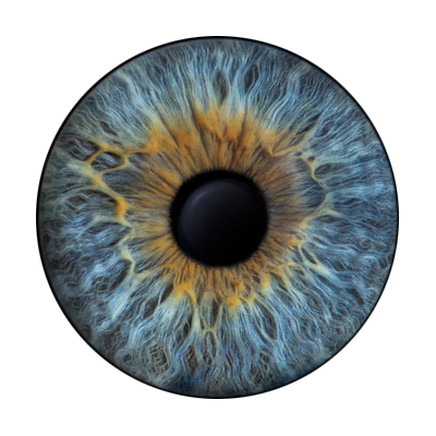
Detecting the tiniest detail...
...to address the
challenges of future
generations
We look closer...

...improves the lives
of millions
Focus by the few...
...helps understand
the bigger picture
Detecting the tiniest detail...
...to address the
challenges of future
generations
We look closer...
...improves the lives of millions
Focus by the few...